The Pros and Cons of Perovskite Solar Cells: The Future of Solar?
For decades, the solar industry has been dominated by one material: silicon. It is reliable, durable, and efficient, forming the bedrock of the global photovoltaic (PV) revolution. However, a new class of materials, known as perovskites, has emerged from research labs with such staggering potential that it promises to reshape the entire industry. In just over a decade, these materials have achieved efficiency gains that took silicon 40 years to reach.
But this remarkable rise is not without its critical flaws. Perovskite solar cells (PSCs) are caught in a classic battle of potential versus practicality. They represent a technology that could lead to ultra-cheap, flexible, and hyper-efficient solar power, yet they are simultaneously plagued by significant challenges in durability, toxicity, and manufacturing scale. This article provides an expert, neutral analysis of the pros and cons of perovskite solar cells, examining whether they are truly the future of solar or a promising technology that may never overcome its own limitations.
What Are Perovskite Solar Cells and How Do They Differ from Silicon?
First, it is essential to understand what “perovskite” means. It is not a single element, like silicon. Instead, a perovskite is a material with a specific crystal structure, named after the mineralogist L.A. Perovski. The most common formula for this structure is ABX3. In a solar cell, this is a compound, often a hybrid of organic and inorganic materials (like methylammonium lead iodide), that serves as the light-harvesting active layer.
The primary difference between a perovskite cell and a conventional silicon cell lies in its structure and manufacturing.
- Silicon cells are made from thick, rigid wafers of highly purified silicon (c-Si). This purification requires extremely high temperatures (over 1400°C) and an energy-intensive process to grow large, defect-free ingots. These ingots are then sliced into wafers, a process that wastes a significant amount of material.
- Perovskite cells are a type of thin-film technology. The active perovskite layer is incredibly thin, often just 0.3 to 0.5 micrometers (µm), which is over 300 times thinner than a typical silicon wafer. This layer can be created at low temperatures (often below 150°C) from a liquid “ink” of precursor chemicals.
Think of it this way: manufacturing a silicon wafer is like carving a perfect statue from a massive, expensive block of marble. Manufacturing a perovskite cell is like using a high-tech printer to “paint” an ultra-thin, functional layer onto a substrate from a low-cost ink. This fundamental difference is the source of both its greatest advantages and its most severe drawbacks.
The “Pros”: Why Perovskites Are a Photovoltaic Game-Changer
The excitement surrounding perovskites is well-founded. They excel in areas where silicon is physically and economically limited, offering a new trajectory for solar technology.
How efficient are perovskite solar cells today?
Perovskite solar cells have demonstrated extraordinary efficiency gains in a remarkably short time. While the first perovskite cell in 2009 had an efficiency of just 3.8%, by 2025, lab-scale research cells have achieved certified efficiencies over 26%, on par with the best monocrystalline silicon cells.
However, the true “game-changer” is not in perovskites alone, but in their use in tandem solar cells. A tandem cell stacks two different solar materials to capture more of the solar spectrum.
- The perovskite layer is “tuned” to absorb high-energy light (like blues and greens).
- The light it doesn’t absorb (like reds and infrared) passes through to the silicon layer below, which is excellent at converting this lower-energy light.
This multi-junction approach shatters the theoretical efficiency limit of single-junction silicon cells (known as the Shockley-Queisser limit, around 29.4%). As of 2025, research teams have already demonstrated perovskite-on-silicon tandem cells with certified efficiencies exceeding 33%, a figure once thought impossible for commercial solar.
Why are perovskites so much cheaper to manufacture?
Perovskite manufacturing is potentially far cheaper because it avoids the massive energy, capital, and material costs associated with silicon. The process, known as solution-based processing, is entirely different.
- Low Energy Input: As mentioned, perovskites are processed at low temperatures. Silicon requires massive furnaces running at over 1400°C. This drastically reduces the energy payback time (EPBT) of the panel.
- Minimal Material: The active layer is hundreds of times thinner than silicon, meaning it requires a tiny fraction of raw material to produce the same power.
- New Manufacturing Methods: Because perovskites start as a liquid ink, they can be deposited using “roll-to-roll” (R2R) printing, similar to how newspapers are printed. This is a continuous, high-speed process, a stark contrast to silicon’s batch-based, slow wafer-slicing method.
The potential cost, once scaled, could be less than half that of conventional silicon panels, though this is purely an estimate until mass production is achieved. These cost estimates vary significantly by region and the final-scaled manufacturing process.
What new applications can perovskites unlock?
Yes, their unique physical properties—being lightweight, thin, flexible, and even semi-transparent—allow perovskites to be used in applications where traditional rigid silicon panels are impractical or impossible.
- Building-Integrated PV (BIPV): Perovskites can be made semi-transparent, allowing them to be coated onto windows and building facades, turning entire skyscrapers into power-generating structures.
- Flexible Solar: The thin-film ink can be printed onto flexible substrates like plastic or metal foils. This enables lightweight, flexible solar panels that can be rolled up, integrated into backpacks, tents, or clothing.
- Niche Electronics & Aerospace: Their high power-to-weight ratio is ideal for powering satellites, high-altitude drones, and electric vehicles, where weight is a critical performance metric.
- Indoor & Low-Light Performance: Perovskites are exceptionally good at harvesting indoor, ambient light from LEDs or fluorescent bulbs, making them perfect for powering small Internet of Things (IoT) sensors and devices without batteries.
The “Cons”: Key Challenges Hindering Mass Adoption
Despite the immense promise, perovskites are not yet on residential rooftops for several critical reasons. These challenges are the focus of billions of dollars in research and development worldwide.
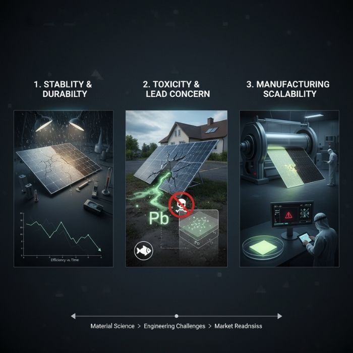
What is the main stability problem with perovskites?
The primary challenge is long-term durability. Perovskite crystal structures, particularly the hybrid organic-inorganic ones, are notoriously unstable and can degrade rapidly when exposed to real-world conditions like moisture, oxygen, heat, and ultraviolet (UV) light.
Unlike silicon, which is an incredibly stable rock, the perovskite material itself can chemically decompose. Moisture can break down the crystal, and heat can cause components to separate, leading to a rapid drop in performance. While silicon panels are warrantied for 25-30 years, early perovskite cells could degrade in days or hours. Researchers are aggressively tackling this with:
- Better “Recipes”: Developing all-inorganic or different organic compound formulas that are more stable.
- Advanced Encapsulation: Creating new, hermetic (airtight) sealing layers to protect the perovskite from the environment.
Until perovskite modules can be proven to survive 20+ years in the field, they cannot compete with silicon in the bankable, long-term residential and utility markets.
Are perovskite solar cells toxic?
Yes, the most efficient and stable perovskite formulas currently contain a small amount of water-soluble lead (Pb). This raises significant environmental, health, and regulatory concerns for a product intended to be “green.”
While the amount of lead in a single panel is very small (often less than a gram, far less than a single car battery), its solubility is the problem. In a standard lead-acid battery, the lead is contained in a thick plastic case. In a perovskite panel, if the panel were to be damaged by hail or in a fire, this soluble lead could potentially leach into groundwater or soil. This is a major barrier to regulatory approval under frameworks like the EU’s Restriction of Hazardous Substances (RoHS) directive.
Researchers are attacking this problem from two angles:
- Lead Sequestration: Designing panels with internal layers that can absorb or “chelate” all the lead, trapping it within the panel even if it’s shattered.
- Lead-Free Alternatives: Actively developing alternative perovskite formulas using other metals, such as tin (Sn). However, tin-based perovskites are currently much less efficient and have even worse stability problems than lead-based ones.
Can perovskite manufacturing be scaled up?
Scaling perovskite production from small, one-centimeter-square “hero” lab cells to large, uniform commercial panels (e.g., two square meters) is a massive engineering hurdle.
The techniques used to achieve record efficiency in a lab (like spin-coating) are not viable for mass production. High-speed, large-area deposition methods like slot-die coating or R2R printing must be perfected. The challenge is achieving a perfectly uniform, pinhole-free crystalline layer over a large surface. A single microscopic defect or impurity in the “ink” can create a “shunt” that short-circuits and deactivates an entire section of the panel, crippling its output.
Perovskite vs. Silicon: A Head-to-Head Comparison
This table summarizes the key differences between today’s mainstream technology (Monocrystalline Silicon) and the emerging challenger (Perovskites) as of 2025.
| Feature | Monocrystalline Silicon (c-Si) | Perovskites (PSC) |
|---|---|---|
| Max Lab Efficiency (Single) | ~26.4% | ~26.1% (Catches up quickly) |
| Max Lab Efficiency (Tandem) | N/A (Is the base layer) | >33% (Perovskite-on-Silicon tandem) |
| Manufacturing Process | High-energy (>1400°C), batch-based, rigid wafer slicing | Low-energy (<150°C), solution-based, “printing” (R2R) |
| Material & Form | Thick (~160 µm), rigid, brittle, heavy | Ultra-thin (<0.5 µm), flexible, lightweight, tunable transparency |
| Long-Term Stability | Excellent. 25-30 year warranted lifespan is standard. | Poor. Highly vulnerable to moisture, oxygen, and heat. |
| Key Disadvantage | High manufacturing cost/energy; physical rigidity. | Poor durability and environmental toxicity (lead). |
The Path to Commercialization and Global Impact
The race to commercialize perovskites is a global one, with research hubs and startups competing to be the first to solve the critical “stability-at-scale” problem.
When will perovskite solar panels be available for homeowners?
While some niche, low-power perovskite products (like indoor IoT sensors) are entering the market in 2025, widespread availability of perovskite-based residential rooftop panels is not expected for several more years, likely closer to 2028-2030 at the earliest.
The most likely route to market for homeowners will be the perovskite-on-silicon tandem cells. These will look and feel like a conventional silicon panel but will be marketed as a “premium” product with a significantly higher efficiency (e.g., 28% or 30% panel efficiency) and a higher price point. Pure perovskite panels, especially flexible or transparent ones, will likely be limited to niche applications (BIPV, automotive, military) before they can meet the 25-year warranty demands of the residential market.
Residential rooftop panels is not expected for several more years, you can see our review of the top 10 best solar panels available on the market today.
What is the role of global research in solving these challenges?
A massive, coordinated global effort is underway to bridge the gap from lab to fab.
- In the United States: The U.S. National Renewable Energy Laboratory (NREL) is a world leader in perovskite research and efficiency certification. The U.S. Department of Energy funds numerous projects, including the “Perovskite Startup Prize,” to accelerate commercialization and solve manufacturing challenges.
- In the European Union: Research consortiums in Germany (e.g., Fraunhofer ISE), Switzerland (EPFL), and the UK (Oxford) are pioneering tandem cell technology and lead-free alternatives, supported by public funds from programs like Horizon Europe.
- In Emerging Markets & Asia: China has a dominant and heavily-funded research program, aiming to corner the next generation of PV manufacturing. Research bodies in India and Türkiye are also actively developing low-cost perovskite formulations, as the technology is seen as a way to achieve energy independence at a lower cost than silicon.
This global competition is rapidly accelerating progress. According to the International Energy Agency (IEA), the continued development of such novel PV technologies is critical to meeting long-term global climate and energy goals. Regional incentives and local regulations, especially concerning lead, will play a huge role in which markets adopt the technology first.
Plot Summary
Perovskite solar cells are arguably the most exciting development in photovoltaics in the last 50 years. They are not a simple, incremental improvement; they represent a fundamentally different and potentially far cheaper way to harness solar energy. However, the hype must be tempered by engineering reality.
Here is a final summary of the core pros and cons:
- The Pros: Perovskites promise extraordinary efficiency (especially in tandem with silicon), exceptionally low manufacturing costs from cheap materials, and a physical flexibility that unlocks new markets like solar windows and lightweight electronics.
- The Cons: They face three critical, non-negotiable hurdles: (1) Durability, as they are not yet proven to last 20+ years; (2) Toxicity, due to the water-soluble lead in their best-performing formulas; and (3) Scalability, as it remains difficult to produce large, uniform, and defect-free panels.
In 2025, it is most accurate to view perovskites not as an immediate replacement for silicon, but as a powerful enhancer. The first perovskite products you are likely to see for sale will be high-efficiency tandem panels, which combine the best of both worlds: perovskite’s efficiency boost with silicon’s proven stability. The long-term future of “pure” perovskite panels hinges entirely on researchers and engineers solving the durability and toxicity crisis.

Solar Energy Enthusiast & Renewable Energy Researcher
Vural’s journey into solar energy began four years ago, driven by frequent power outages and high electricity bills at his own home. He has since gained hands-on experience with both personal and commercial solar projects. At solarpanelresource.com, Vural shares his real-world insights and in-depth research to guide homeowners and business owners on their own path to energy independence.